(China (Mainland))

Product Summary
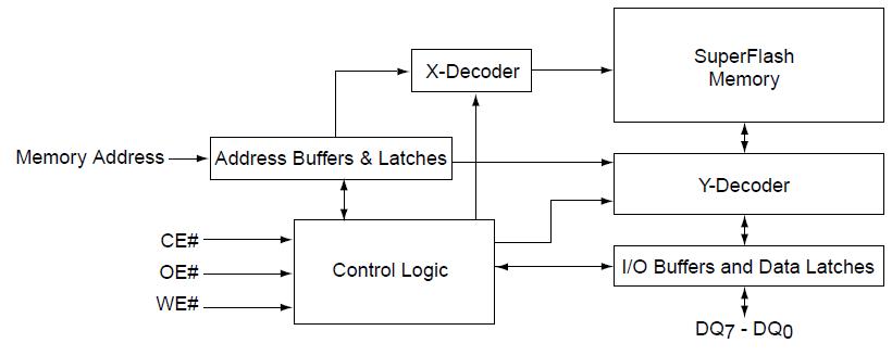
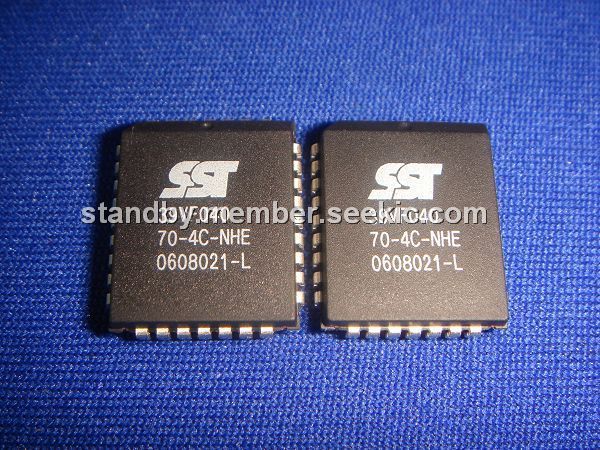
The 39VF040 is a 512 Kbit/1 Mbit/2 Mbit/4 Mbit (x8) CMOS Multi-Purpose Flash (MPF) manufactured with SST’s proprietary, high performance CMOS SuperFlash technology. The split-gate cell design and thick oxide tunneling injector attain better reliability and manufacturability compared with alternate approaches. The 39VF040 writes with a 2.7-3.6V power supply. The device conforms to JEDEC standard pinouts for x8 memories. Featuring high performance Byte-Program, the 39VF040 provides a maximum Byte-Program time of 20μsec. The device uses Toggle Bit or Data# Polling to indicate the completion of Program operation.
Parametrics
39VF040 absolute maximum ratings: (1)Temperature Under Bias: -55℃ to +125℃; (2)Storage Temperature: -65℃ to +150℃; (3)D. C. Voltage on Any Pin to Ground Potential: -0.5V to VDD + 0.5V; (4)Transient Voltage (<20 ns) on Any Pin to Ground Potential: -1.0V to VDD + 1.0V; (5)Voltage on A9 Pin to Ground Potential: -0.5V to 13.2V; (6)Package Power Dissipation Capability (Ta = 25℃): 1.0W; (7)Output Short Circuit Current1: 50 mA.
Features
39VF040 features: (1)Organized as 64K x8 / 128K x8 / 256K x8 / 512K x8; (2)Single Voltage Read and Write Operations: 2.7-3.6V; (3)Superior Reliability, Endurance: 100,000 Cycles (typical); Greater than 100 years Data Retention; (4)Superior Reliability, Endurance: 100,000 Cycles (typical); Greater than 100 years Data Retention; (5)Sector-Erase Capability, Uniform 4 KByte sectors; (6)Fast Read Access Time: 70 and 90 ns; (7)Latched Address and Data; (8)Fast Erase and Byte-Program: Sector-Erase Time: 18 ms (typical); Chip-Erase Time: 70 ms (typical); Byte-Program Time: 14 μs (typical); Chip Rewrite Time: 8 seconds (typical); (9)Automatic Write Timing: Internal VPP Generation; (10)End-of-Write Detection; (11)CMOS I/O Compatibility; (12)JEDEC Standard, Flash EEPROM Pinouts and command sets; (13)Packages Available: 32-lead PLCC.
Diagrams