(China (Mainland))

Product Summary
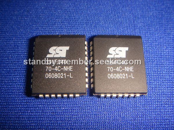
The 39VF040-70-4C-NHE is a is a CMOS Multi-Purpose Flash (MPF). It is manufactured with SST proprietary, high performance CMOS SuperFlash technology. The 39VF040-70-4C-NHE uses Toggle Bit or Data# Polling to indicate the completion of Program operation. To protect against inadvertent write, it has on-chip hardware and Software Data Protection schemes. The 39VF040-70-4C-NHE is suited for applications that require convenient and economical updating of program, configuration, or data memory.
Parametrics
39VF040-70-4C-NHE absolute maximum ratings: (1)Temperature Under Bias: -55℃ to +125℃; (2)Storage Temperature: -65℃ to +150℃; (3)D. C. Voltage on Any Pin to Ground Potential: -0.5V to VDD+0.5V; (4)Transient Voltage (<20 ns) on Any Pin to Ground Potential: -2.0V to VDD+2.0V; (5)Voltage on A9 Pin to Ground Potential: -0.5V to 13.2V; (6)Package Power Dissipation Capability (Ta = 25℃): 1.0W; (7)Surface Mount Solder Reflow Temperature: 260℃ for 10 seconds; (8)Output Short Circuit Current: 50 mA.
Features
39VF040-70-4C-NHE features: (1)Organized as 64K x8 / 128K x8 / 256K x8 / 512K x8; (2)Single Voltage Read and Write Operations; (3)Superior Reliability: Endurance: 100,000 Cycles (typical), Greater than 100 years Data Retention; (4)Low Power Consumption(typical values at 14 MHz): Active Current: 5 mA (typical), Standby Current: 1 μA (typical); (5)Sector-Erase Capability: Uniform 4 KByte sectors; (6)Fast Read Access Time: 70 and 90 ns; (7)Latched Address and Data; (8)Fast Erase and Byte-Program: Sector-Erase Time: 18 ms (typical), Chip-Erase Time: 70 ms (typical), Byte-Program Time: 14 μs (typical), Chip Rewrite Time: 8 seconds (typical); (9)Automatic Write Timing: Internal VPP Generation; (10)End-of-Write Detection: Toggle Bit, Data# Polling; (11)CMOS I/O Compatibility; (12)JEDEC Standard:Flash EEPROM Pinouts and command sets.
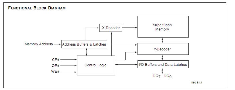
Diagrams